Digital Baseband-Modem
Dual-Mode Baseband-Modem
The Dual-Mode Baseband-Modem (BM) is responsible for handling the transmission and reception of both Bluetooth LE and IEEE 802.15.4 packets. For Bluetooth Low Energy, the BM handles Bluetooth Low Energy 1M Uncoded Link Layer Packets. For IEEE 802.15.4, the BM handles packets transmitted according to the PHY standard for the O-QPSK modulation in the 2.4 GHz band. Additionally the BM exposes an interface for the CPU to read/write various information (e.g. tuning bits) to the analog RF.
There are two primary sub-components in the Baseband-Modem, the Baseband, and the Modem. The baseband is responsible for the bit-stream processing of incoming and outgoing packets. The modem is responsible for modulation on the TX side, and digital image rejection and demodulation on the RX side.
Architecture Overview
Baseband-Modem Frontend
Commands and MMIO Registers
The baseband-modem (BM) block contains a set of memory mapped registers used for passing commands to the BM, tuning analog RF components, and making BM status visible to the CPU. The address map is shown below. Note that the addresses are relative to the BM’s base attachment address. For example, if the BM is attached at 0x8000, then the address of 0x04 corresponds to 0x8004.
| ADDR | DATA | Size (bits) | Description |
|---|---|---|---|
| 0x00 | Instruction | 32 | Instruction received from processor. Contains 4 bits of primary instruction, 4 bits of secondary instruction, then 24 bits of data. |
| 0x04 | Additional Data | 32 | Additional data to write. Set data before writing instructions when applicable. |
| 0x08 | Status 0 | 32 | [2:0] Assembler State [5:3] Disassembler State [7:6] TX State [10:8] RX Controller State [12:11] TX Controller State [15:13] Controller State [23:16] ADC I data [31:24] ADC Q data |
| 0x0C | Status 1 | 32 | [5:0] Modulation LUT index [10:6] I AGC LUT index [15:11] I DCOC LUT index [20:16] Q AGC LUT index [25:21] Q DCOC LUT index |
| 0x10 | Status 2 | 32 | [31:0] BLE CDR bit count |
| 0x14 | Status 3 | 32 | [31:0] LRWPAN CDR bit count |
| 0x18 | Status 4 | 32 | [31:0] LO/32 counter |
| 0x1C | General trim 0 | 8 | General trim bits (N/C) |
| 0x1D | General trim 1 | 8 | [0] LO/32 input (external, not implemented) |
| 0x1E | General trim 2 | 8 | General trim bits (N/C) |
| 0x1F | General trim 3 | 8 | General trim bits (N/C) |
| 0x20 | General trim 4 | 8 | General trim bits (N/C) |
| 0x21 | General trim 5 | 8 | General trim bits (N/C) |
| 0x22 | General trim 6 | 8 | General trim bits (N/C) |
| 0x23 | General trim 7 | 8 | Debug Enable (0 = debug enable) |
| 0x24 | I VGA gain control | 10 | Manual VGA value if not using I AGC |
| 0x26 | I VGA attenuation reset | 1 | reset the I AGC |
| 0x27 | I VGA attenuation useAGC | 1 | use I AGC (manual VGA value if not) |
| 0x28 | I VGA attenuation sample window | 8 | I AGC sample window |
| 0x29 | I VGA attenuation ideal peak to peak | 8 | I AGC ideal peak to peak |
| 0x2A | I VGA tolerance peak to peak | 8 | I AGC peak to peak tolerance |
| 0x2B | I BPF CHP 0 & 1 | 8 | I bandpass filter tuning |
| 0x2C | I BPF CHP 2 & 3 | 8 | I bandpass filter tuning |
| 0x2D | I BPF CHP 4 & 5 | 8 | I bandpass filter tuning |
| 0x2E | I BPF CLP 0 & 1 | 8 | I bandpass filter tuning |
| 0x2F | I BPF CLP 2 | 4 | I bandpass filter tuning |
| 0x30 | Q VGA gain control | 10 | Manual VGA value if not using Q AGC |
| 0x32 | Q VGA attenuation reset | 1 | reset the Q AGC |
| 0x33 | Q VGA attenuation useAGC | 1 | use Q AGC (manual VGA value if not) |
| 0x34 | Q VGA attenuation sample window | 8 | Q AGC sample window |
| 0x35 | Q VGA attenuation ideal peak to peak | 8 | Q AGC ideal peak to peak |
| 0x36 | Q VGA tolerance peak to peak | 8 | Q AGC peak to peak tolerance |
| 0x37 | Q BPF CHP 0 & 1 | 8 | Q bandpass filter tuning |
| 0x38 | Q BPF CHP 2 & 3 | 8 | Q bandpass filter tuning |
| 0x39 | Q BPF CHP 4 & 5 | 8 | Q bandpass filter tuning |
| 0x3A | Q BPF CLP 0 & 1 | 8 | Q bandpass filter tuning |
| 0x3B | Q BPF CLP 2 | 4 | Q bandpass filter tuning |
| 0x3C | I DCO use | 1 | toggle using I DCO |
| 0x3D | I DCO reset | 1 | reset the I DCO |
| 0x3E | I DCO gain | 8 | set gain for I DCO (unsigned FixedPoint w/ 2 bit binary point) |
| 0x3F | Q DCO use | 1 | toggle using Q DCO |
| 0x40 | Q DCO reset | 1 | reset the Q DCO |
| 0x41 | Q DCO gain | 8 | set gain for Q DCO (unsigned FixedPoint w/ 2 bit binary point) |
| 0x42 | DCOC tuning 1 | 6 | Manual I current DAC for stage 2 VGA value if not using I DCO |
| 0x43 | DCOC tuning 2 | 6 | Manual Q current DAC for stage 2 VGA value if not using Q DCO |
| 0x46 | MUX debug in | 10 | Debug configuration, input |
| 0x48 | MUX debug out | 10 | Debug configuration, output |
| 0x4A | Enable RX I | 5 | Manual enable RX I values {3’b0, mix, buf, vga_s1, vga_s2, bpf} |
| 0x4B | Enable RX Q | 5 | Manual enable RX Q values {3’b0, mix, buf, vga_s1, vga_s2, bpf} |
| 0x4C | Enable VCO LO | 2 | Manual enable VCO LO {6’b0, vco_lo, lna} |
| 0x50 | LUT command | 32 | LUT set instruction [3:0] LUT ID [9:4] address (index) [31:10] value |
| 0x54 | RX error message | 32 | Interrupt message, RX error message |
| 0x58 | RX finish message | 32 | Interrupt message, RX finish message |
| 0x5C | TX error message | 32 | Interrupt message, TX error message |
| 0x60 | FIR command | 32 | FIR filter reprogramming instruction, [3:0] FIR ID [9:4] coefficient (index) [31:10] value |
| 0x64 | I VGA attenuation gain increase | 8 | I AGC gain increase step size (by LUT index) |
| 0x65 | I VGA attenuation gain decrease | 8 | I AGC gain decrease step size (by LUT index) |
| 0x66 | Q VGA attenuation gain increase | 8 | Q AGC gain increase step size (by LUT index) |
| 0x67 | Q VGA attenuation gain decrease | 8 | Q AGC gain decrease step size (by LUT index) |
The processor should always write to the additional data register prior to writing to the instruction register for a given command. Writing to the register at 0x00 is the trigger for the BM to execute a given command.
In order to pass commands to the BM, two 32-bit registers at addresses 0x00 and 0x04 are utilized. The register at 0x04 contains the additional data field for a given command while the register at 0x00 contains the instruction.
The format for a BM instruction is:
| Bits | 31-8 | 7-4 | 3-0 |
|---|---|---|---|
| Field | Data | Instruction 2 | Instruction 1 |
List of Commands
Configure Command
Configure baseband constants. The constant is selected using the instruction 2 field and set to the value specified in the additional data field. In the case that the secondary instruction is set to CONFIG_LUT, reference the LUT addresses provided in the explanations below.
| Field | Data | Instruction 2 | Instruction 1 |
|---|---|---|---|
| Value | X unless CONFIG_LUT, then LUT address | See table | 0 |
| Field | Additional Data |
|---|---|
| Value | Value for the constant to be set to |
| Instruction 2 | Name |
|---|---|
| 0x0 | CONFIG_RADIO_MODE |
| 0x1 | CONFIG_CRC_SEED |
| 0x2 | CONFIG_ACCESS_ADDRESS |
| 0x3 | CONFIG_SHR |
| 0x4 | CONFIG_BLE_CHANNEL_INDEX |
| 0x5 | CONFIG_LRWPAN_CHANNEL_INDEX |
Configuration instruction descriptions
(0x0) CONFIG_RADIO_MODE: Specify the following in the Additional Data register (0x04) prior to issuing the instruction
- 0: Set the radio transceiver mode to Bluetooth Low Energy
- 1: Set the radio transceiver mode to IEEE 802.15.4 LR-WPAN
Valid in any radio mode.
(0x1) CONFIG_CRC_SEED: Set the CRC (cyclic redundancy check) seed for the BLE and LR-WPAN CRC circuits to the value in the Additional Data register (0x04). This value changes for BLE and should be 0 for LR-WPAN
(0x2) CONFIG_ACCESS_ADDRESS: Set the BLE Access Address for the BLE uncoded packet. This value must be provided by the CPU. More information may be found in the BLE Baseband section.
An access address of 0xFFFFFFF6 disables whitening of transmitted BLE packets
(0x3) CONFIG_SHR: Set the LRWPAN SHR to match with for receiving a LRWPAN packet. This value must be provided by the CPU. According to 802.15.4 spec, it should be a fixed value of 0xA700 (only 2 bytes are matched due to lower hardware cost), but is programmable for flexibility.
(0x4) CONFIG_BLE_CHANNEL_INDEX: Values for the channel index can range from 0 to 39, corresponding to BLE channel frequencies beginning at 2402 MHz until 2480 MHz. It is critical to note that the channel index from 0 to 39 is a direct mapping to channel frequencies - NOT the BLE channel numbering scheme that considers advertising channels separately. For example, setting CONFIG_BLE_CHANNEL_INDEX to 0 will result in a transmission with center frequency at 2402 MHz. This corresponds to BLE channel 37. More information
(0x5) CONFIG_LRWPAN_CHANNEL_INDEX: Values for the channel index can range from 0 to 15, corresponding to LR-WPAN channel frequencies beginning at 2405 MHz until 2480 MHz.
Send Command
Transmit a specified number of PDU header and data bytes. Bytes are retrieved by the BM by loading them from the specified address.
| Field | Data | Instruction 2 | Instruction 1 |
|---|---|---|---|
| Value | Number of bytes | X | 1 |
| Field | Additional Data |
|---|---|
| Value | Load address |
Receive Enter Command
Place the device into receive mode. If a message is picked up, it will be stored starting at the specified address address.
| Field | Data | Instruction 2 | Instruction 1 |
|---|---|---|---|
| Value | X | X | 2 |
| Field | Additional Data |
|---|---|
| Value | Storage address |
Receive Exit Command
Exit the device from receive mode. This command will succeed as long as the device has not yet matched an instruction preamble.
| Field | Data | Instruction 2 | Instruction 1 |
|---|---|---|---|
| Value | X | X | 3 |
| Field | Additional Data |
|---|---|
| Value | X |
Debug Command
Turns on both the TX and RX paths according to the specified loopback mask before passing the specified number of PDU bytes in a loop. For simplicity the return data is stored at <load address + total bytes> rounded to the next byte aligned address. The loopback mask is used to determine at which point the data should be revered and sent back towards the CC.
| Field | Data | Instruction 2 | Instruction 1 |
|---|---|---|---|
| Value | Total bytes to send | Loopback mask | 15 |
| Field | Additional Data |
|---|---|
| Value | Load address and base for store address calculation |
| Loopback Mask | Loopback Point |
|---|---|
| 0b0001 (0x1) | Empty |
| 0b0010 (0x2) | In the modem, loop the FSKTX output back in to the CDR in FSKRX |
| 0b0100 (0x4) | Empty |
| 0b1000 (0x8) | Empty |
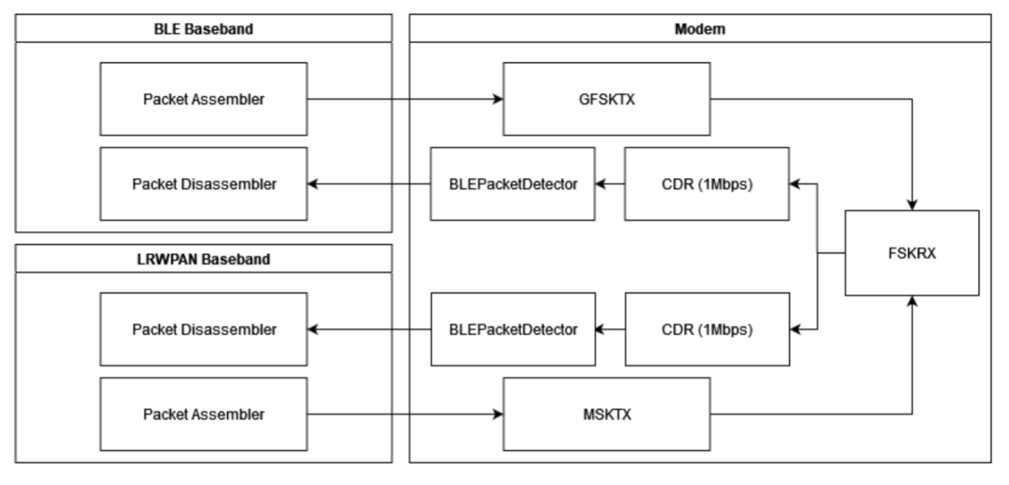
Loopback diagram: Note that the FSKRX module handles loopback logic and directs the output of MSKTX & GFSK TX modules to respective CDR blocks
Configuring Modem LUTs
The modem LUTs can be configured using the LUT command register in the MMIO map enumerated above (register offset 0x50).
LUT IDs are defined as follows:
0x0 - VCO_MOD: 64-entry, 8-bit valued LUT that is sampled to produce frequency deviations from the center frequency. This LUT must be reloaded on each channel and mode change. 0 indicates the largest negative frequency deviation, 63 indicates the largest positive deviation, and 31 indicates no frequency deviation. Note that 0/63 should be +/-250kHz for BLE and +/-500kHz for LR-WPAN.
0x1 - VCO_CT_BLE: 40-entry LUT sampled with BLE channel index to produce coarse and medium tuning bits to drive the VCO to the center frequency of the BLE channel index selected. Does not apply when in LR-WPAN radio mode.
0x2 - VCO_CT_LRWPAN: 16-entry LUT that is sampled with the LR-WPAN channel index to produce the coarse and medium tuning bits to drive the VCO to the center frequency of the LR-WPAN channel index selected. Does not apply when in BLE radio mode.
0x3 - AGC_I: 64-entry LUT that is sampled to drive the VGA attenuation gain for the I channel VGA. Only the lower 32 entries are used.
0x4 - AGC_Q: 64-entry LUT that is sampled to drive the VGA attenuation gain for the Q channel VGA. Only the lower 32 entries are used.
0x5 - DCO_I: 64-entry LUT that is sampled to drive the current DAC for the I channel stage 2 VGA. Only the lower 32 entries are used.
0x6 - DCO_Q: 64-entry LUT that is sampled to drive the current DAC for the Q channel stage 2 VGA. Only the lower 32 entries are used.
Configuring the FIR filter coefficients
The FIR filter coefficients can be configured using the FIR command register in the MMIO map enumerated above (register offset 0x60).
FIR IDs are defined as follows:
0x0 - NONE: Reserved
0x1 - TX_GAUSSIAN: 24-entry, 8-bit FixedPoint (2-bit fractional component) filter for BLE GFSK. Only 16 coefficients are used. Note the filter was designed to run at 8MHz (length = 2*cycles/bit) but there’s a bug in the implementation. The short-term fix to get it working was to double the coefficients.
0x2 - RX_HILBERT_I: 32-entry, 16-bit FixedPoint (12-bit fractional component) filter for image rejection.
0x3 - RX_HILBERT_Q: 32-entry, 16-bit FixedPoint (12-bit fractional component) filter for image rejection. The output of the I and Q filters are summed to form the image rejected signal suitable for FSK demodulation.
0x4 - RX_MATCH_SIN_F0: 32-entry, 16-bit FixedPoint (12-bit fractional component) filter for matched filter for binary 0. Two templates (filters) are used to account for phase shift. Note BLE coefficients are loaded by default. LR-WPAN ones must be loaded separately.
0x5 - RX_MATCH_COS_F0: 32-entry, 16-bit FixedPoint (12-bit fractional component) filter for matched filter for binary 0. Two templates (filters) are used to account for phase shift. Note BLE coefficients are loaded by default. LR-WPAN ones must be loaded separately.
0x6 - RX_MATCH_SIN_F1: 32-entry, 16-bit FixedPoint (12-bit fractional component) filter for matched filter for binary 1. Two templates (filters) are used to account for phase shift. Note BLE coefficients are loaded by default. LR-WPAN ones must be loaded separately.
0x7 - RX_MATCH_COS_F1: 32-entry, 16-bit FixedPoint (12-bit fractional component) filter for matched filter for binary 1. Two templates (filters) are used to account for phase shift. Note BLE coefficients are loaded by default. LR-WPAN ones must be loaded separately.
0x8 - RX_LPF: 32-entry, 16-bit FixedPoint (12-bit fractional component) filter for bitrate filter of the matched filter output. Two filters with the same coefficients are used, one for 0s and another for 1s. Note BLE coefficients are loaded by default. LR-WPAN ones must be loaded separately.
Interrupts
The Baseband-Modem provides five interrupts as outputs from the Baseband Frontend. These interrupts provide the CPU with triggers for events from the transceiver module. The interrupts are described in the table below:
Baseband-Modem interrupt table
| Interrupt Index | Name | Description |
|---|---|---|
| 0 | RX_ERROR | Triggers on recognition of an error while the BM is in RX state. The MMIO register 0x54 will be populated with an RX_ERROR_MESSAGE. Presently not implemented. |
| 1 | RX_START | Triggers when the baseband disassembler/correlator enters the busy state. Denotes that a packet has been received and demodulated, but has not yet been disassembled. |
| 2 | RX_FINISH | Triggers when the disassembler has completed processing an incoming message. Populates the MMIO register RX_FINISH_MESSAGE at 0x58 with the length of the message. |
| 3 | TX_ERROR | Triggers on recognition of an error while the BM is in TX state. The MMIO register 0x5C will be populated with an TX_ERROR_MESSAGE. Presently not implemented. |
| 4 | TX_FINISH | Triggers when the modem has completed transmission of all bytes in the provided message. The DMA read response bytes must match the number of bytes specified in the Send Command for this interrupt to fire. |
IEEE 802.15.4 LR-WPAN Baseband
Baseband modulation/demodulation diagram
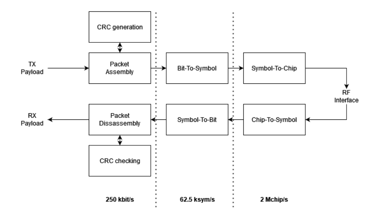
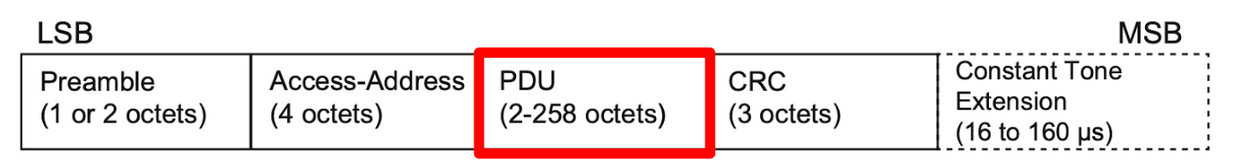
The LR-WPAN baseband transmission chain involves DMA packet disassembly, LR-WPAN packet assembly, CRC generation, bit-to-symbol translation, and symbol-to-chip translation before the final chip stream is provided to the modem for modulation. The packet is assembled according to the IEEE 802.15.4 (LR-WPAN) PPDU schematic (shown below).
It is important to note the rates at each stage of the baseband TX chain. The standard calls for a 250 kb/s bitrate corresponding to packet assembly/packet disassembly. Following bit-to-symbol translation, the symbol rate becomes 62.5 ksym/s (where 4 bits specifies 1 symbol). Following symbol-to-chip translation, the chip rate now matches the LR-WPAN nominal baseband frequency of 2 MHz frequency or 2 Mchip/s (where 1 symbol specifies 32 chips). The inverse applies for the RX chain.
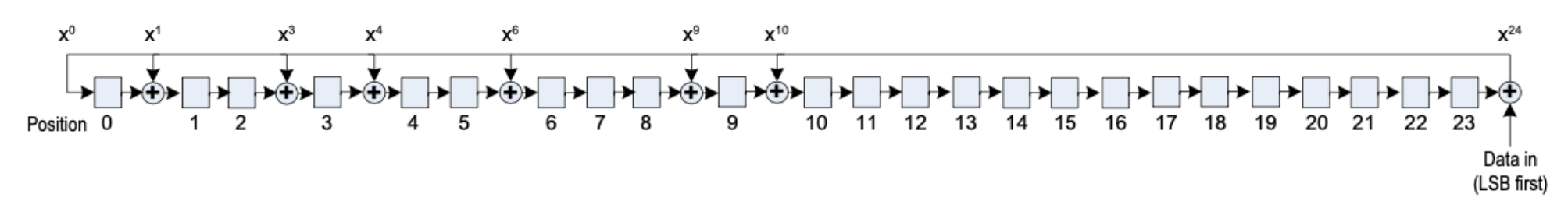
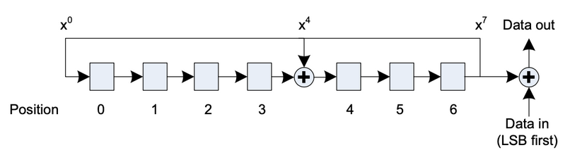
During packet assembly, a frame check sequence is calculated as a 16-bit ITU-T CRC.
CRC calculation diagram
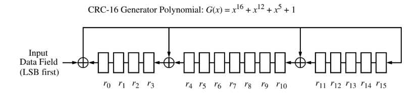
The algorithm for the CRC begins by setting all remainder registers, r0…r15, to zero. Next, we start from the LSB and shift the MHR and payload into the divider. The FCS is then the remainder register after the last bit of the data is shifted in. Lastly, the FCS is appended to the data field so that register r0 is transmitted first.
IEEE 802.15.4 PPDU Schematic
The frame check sequence (FCS) is appended to the end of the PPDU as the MAC footer (MFR) in the diagram above. If the result of CRC checking is false, the [flag] is set to high, before triggering a RX_ERROR message.
PSDU Schematic
The preamble for 15.4 is a 32-bit sequence of all zeros. The SFD is loosely analogous to the Access-Address (AA) of the BLE Baseband in that they both uniquely identify the start of the packet for the protocol used.
Bluetooth Low Energy (BLE) Baseband
BLE baseband and modulation/demodulation diagram
Below is the BLE Uncoded Packet format. All elements of the packet either are or depend on data that the CPU must set (which is taken care of by the SW implementation of the Link Layer). These values are communicated to the packet assembler and disassembler through the controller via the command system over MMIO.
BLE PPDU Schematic
The Preamble is an alternating series of 1s and 0s that depends on the LSB of the Access-Address (AA). The CPU need not provide any additional control signals for this part of the packet.
The Access-Address is a special value set by the SW Link Layer that determines whether a packet is valid or not. This value must be provided by the CPU and depends on past communications or may be set to some default value.
The PDU is the already encrypted content of the packet, the CPU must provide this in its entirety. Through the DMA controller, the packet assembler will retrieve this from main memory. The packet disassembler will deliver a PDU to the main memory once one is received.
The CRC (cyclic redundancy check) is derived from the Link Layer state (which must be provided by the CPU via MMIO register). In the receive chain, if the calculated CRC does not match the CRC found in the PDU, the [flag] is set to high.
BLE CRC functional schematic
Whitening
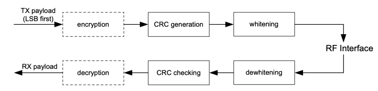
In order to avoid long continuous sequences of 1s and 0s in the transmitted data, the entire packet goes through a process known as whitening.
Whitening diagram
Outgoing data on the TX chain is whitened and incoming data is also “de-whitened”
Unified FSK Modem
The modem sits between the digital baseband and the ADCs / DAC to analog RF. It is responsible for performing demodulation and modulation and clock and data recovery at a rate of 1Mbps for BLE or 2Mchip/s for LR-WPAN. Each cycle, the digital baseband either receives a new bit from the demodulator, or provides a new bit for transmission to the modulator.
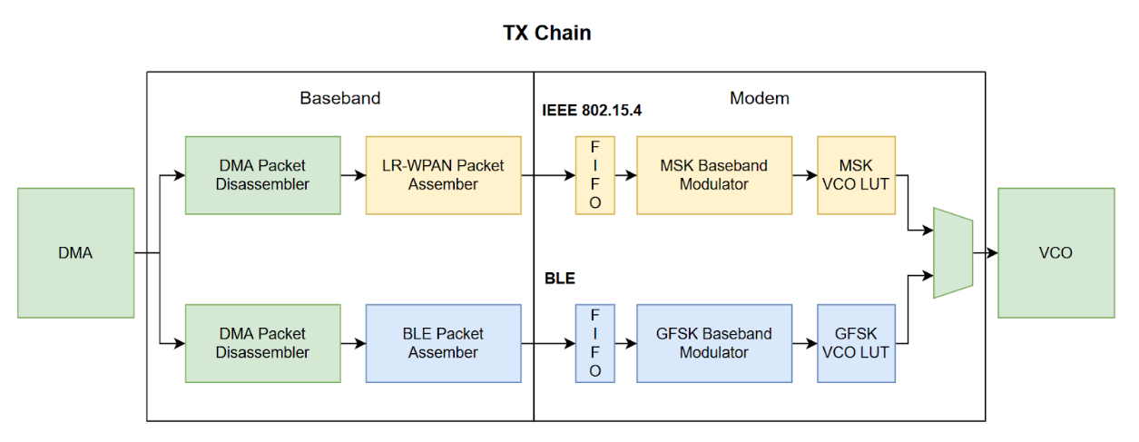
TX Chain
Modem TX chain schematic
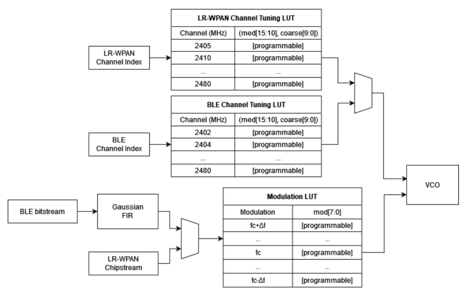
The digital baseband bit-stream process outputs individual bits into a FIFO that will be consumed by the modem for use in modulation. For BLE transmissions, the bitstream is modulated using Gaussian frequency shift keying (GFSK). The modulator modulates the outgoing bits using at a rate of 1Msym/s, with a modulation index of 0.5. For LR-WPAN transmissions, the chipstream directly drives the modulation LUT. The output of the modulation LUT is an 8-bit unsigned integer value that indicates the FSK modulation away from the maximum frequency at that channel tuning.
The 6-bit FSK modulation output, in conjunction with a 6 bit channel select value, are used to address into the Modulation LUT to retrieve input values for the VCO LO based on the channel index and modulation frequency offset. These decoding LUTs provide 8-bit values for LO coarse tuning, LO FSK, and the PLL division.
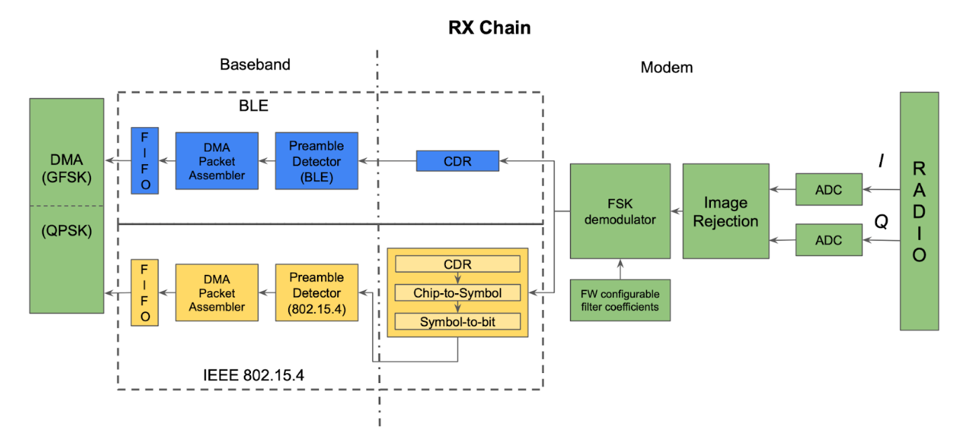
RX Chain
Modem RX chain schematic
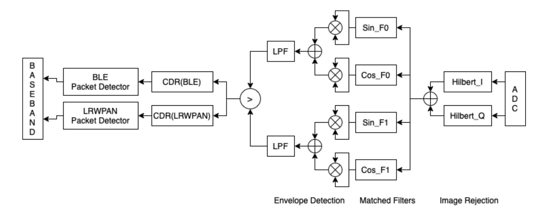
After mixing, the analog I and Q signals go through ADCs to produce 8 bit output values. The ADCs are clocked on the negative edge of the digital system clock. On the falling system clock edge, the ADCs sample and latch the signals coming from analog RF. These sampled 8-bit values are then captured by rising-edge triggered flip-flops at the analog-digital boundary of the RX chain.
Image Rejection
After mixing with the LO and being sampled by the I/Q ADCs, the Q signal for the signal (F_LO+F_IF) ends up +90° shifted from I while the image (F_LO-F_IF) ends up -90° shifted from I. A Hilbert filter shifts positive frequencies by +90° and negative frequencies by -90°. By applying it to the I signal and adding to the Q signal, this causes constructive interference for the desired signal and destructive interference for the image, heavily attenuating it. Note these filters are fully configurable (up to their maximum length) if needed.
FSK Demodulation
After image rejection, the matched filters (the optimal non-coherent demodulator!) and envelope detection serve to discriminate between positive and negative frequency deviations. A matched filter performs a convolution of the input signal with a “template” which is simply samples of the desired frequency up to the length of a bit/chip period. Due to phase shift, we must have sine and cosine templates and sum the two. Since the filters generate high frequency noise, we perform “envelope detection” after the matched filters to remove it and get a clean signal giving the magnitude of the match. Comparing the magnitude of each gives us the decision for the deviation.
For an ADC clock of 32MHz, we need a 32-length filter for BLE and 16-length filter for LR-WPAN. For an IF of 2MHz, we need templates of 1.75MHz and 2.25MHz for BLE and 1.5MHz and 2.5MHz for LR-WPAN.
Clock and Data Recovery (CDR)
After FSK demodulation, we have an oversampled bitstream which must downsample to the appropriate bitrate. The goal of the CDR is to align the sampling window with the phase of the incoming bitstream.
Our design has 3 integrators - early, present, late - which each look at a window (of length equal to the bit period) of the incoming bitstream but are offset from each other by 1 cycle. We then have a counter that decrements every cycle. When the counter hits 0, we return a sampled bit that is the value of the strongest integrator (determined by majority and number of 1s and 0s). We then reset the counter to a value that will cause the winning integrator in the next bit period to be closer to the present integrator (either by extending or shortening the amount of time to the next sample time).
Automatic Gain Control (AGC)
The AGC supports a high dynamic range by keeping the ADCs near saturation. It tracks the minimum and maximum ADC values and increases or decreases the gain based on signal strength. It is recommended to keep the tolerance larger than the gain resolution to prevent oscillation.
DC Offset Compensation (DCO)
The DCO integrates the incoming signal, applies gain, and feeds back into the LUT to calibrate the VGA and remove DC offset.
Example Radio Front-End (RFE)
The example RFE operates in the 2.4G to 2.4835 GHz range, covering 70 1MHz RF channels. The receive chain functions from -70dBm to -10dBm with detailed interference specifications for in-band and out-of-band conditions. It uses a low-IF receiver and direct modulation transmitter architecture.