Digital Core
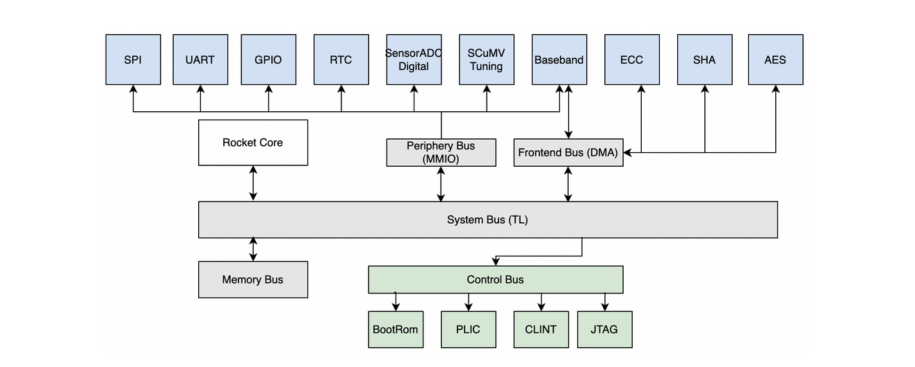
Key Features
- RV32IMAFC Single Rocket Core
- 3 clocks for CPU core and peripherals:
- 200 MHz CPU clock
- 32 MHz ADC clock for BLE/IEEE 802.15.4 baseband-modem and precision sigma-delta ADC
- 1MHz RTC clock
- On-chip SRAM
- 256kB scratchpad (“L2”)
- 8kB 2 way I & D
- JTAG, UART, QSPI Flash, GPIO
- Interrupt controller
- PLIC (platform level)
- CLINT (core level)
- RTC capture and compare peripheral
Power Consumption
Power consumption comparison of the core running a program with baseband register read/write and ALU usage. VCC=0.85V, CPU clock=200MHz
| Internal Power (mW) | Switching Power (mW) | Leakage Power (mW) | Total Power (mW) | |
|---|---|---|---|---|
| SCuM-V22 in Lab | 11.9 | - | 36 | 42.5 |
| SCuM-V23 dynamic power simulation | 7.9 | 3.2 | 0.060 | 11.2 |
Based on simulations, total power consumption of the core decreased by 73% from SCuM-V22 to SCuM-V24B. This improvement was achieved by reducing leakage power in the SRAM cells.
Boot Process
| Method | BOOT_SEL Value | Boot Address | Interface | Boot Process Description |
|---|---|---|---|---|
| Self Boot | 1 | 0x2000_0000 | SPI | SPI flash content is copied to memory Jump to self boot base address |
| Tethered Boot | 0 | 0x0000_0000 | TSI & JTAG | 1. Boot ROM configures a trap handler, and enters a wait for interrupt loop. 2. Use JTAG, TSI, or other external debugging tools to program the on-chip memory 3. Use JTAG, TSI, or other external tools to trigger a software interrupt (MSIP) 4. Boot ROM handles interrupt, jumps to the program memory. |