Power System
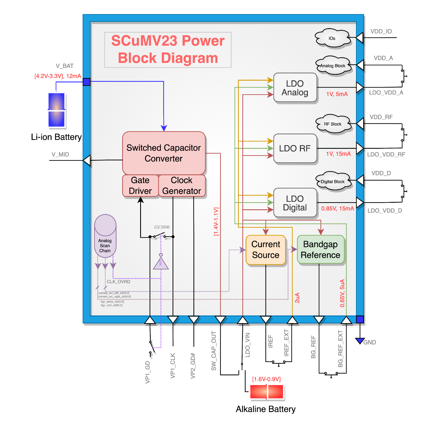
SCuM-V24B has 3 power domains:
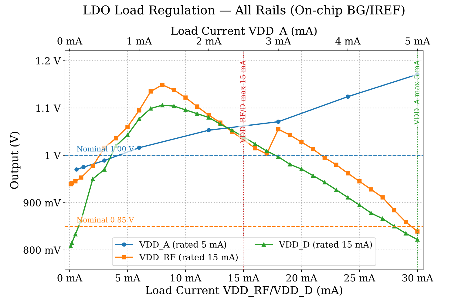
- VDD_A - 1V, 5mA expected
- VDD_RF - 1V, 15mA expected
- VDD_D - 0.85V, 15mA expected
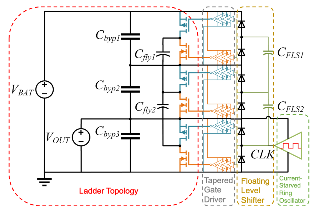
Switched Capacitor Converter
Ladder 3:1 Topology
- All capacitors & switches are rated at Vout.
- Externally Reconfigurable for 3:1, 2:1, 3:2 for exploiting full battery voltage range.
Switched capacitor converter schematic:
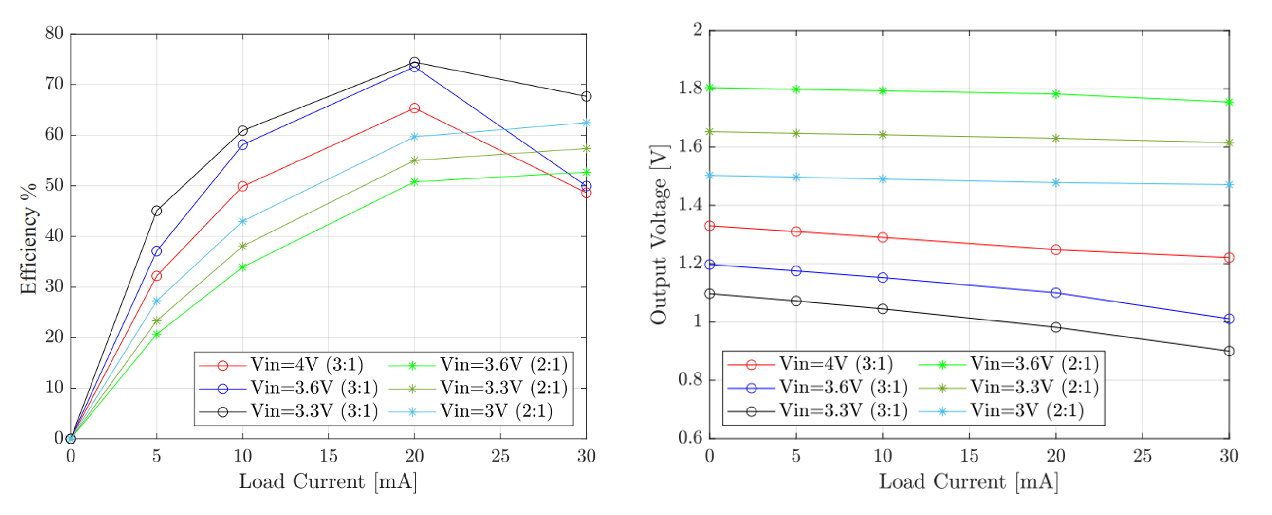
Simulated Efficiency Variation with Load
(Left) Efficiency Variation with Load. (Right) Vout Variation with Load:
Simulated performance
| Simulated Performance Parameters | Details |
|---|---|
| Clock Frequency | 85MHz-120MHz |
| Peak Power Efficiency | 75% (Pre-layout) |
| Full-load Efficiency | 68% (Pre-layout) and <50% (Post-layout) |
| Max Vout_ripple (pk-pk) | 50 mVpp |
| Power Density at full-load | 65mW/mm² @100MHz |
Overview of High-Level Power Converter Design
| Parameters | Details |
|---|---|
| Total Capacitance | 6.5nF |
| Capacitor Type | MOM+MOS |
| Vin Range | 4.2 V-3V |
| Vout Range | 1.8V-1.1V |
| Conversion Ratios | 3:1, 2:1 |
| Load Range | 5mA to 30mA |
| Switched-Capacitor Area | 450,000 um² (75% of Power Block) |
| Max Output Power | 30 mW |
Low Dropout (LDO) Voltage Regulators
The design of the LDO is a 2-stage amplifier where the output of the differential amplifier drives the gate of the PMOS at the second stage and the output of the drain of this PMOS is the regulated voltage. This voltage is then passed through a resistor-feedback network to get the desired regulated voltage for different power domains. An additional capacitor is attached at the output voltage as well to stabilize the LDO. Since each domain requires different voltages, the resistors values were chosen to such that the feedback yielded the desired voltage for different domains (1V for the RF analog, and 0.85V for Digital).
Simulated performance
| Parameter | LDO_RF (1 V) | LDO_Digital (0.85 V) | LDO_Analog (1 V) |
|---|---|---|---|
| Vin | 1.8 V - 1.2 V | 1.8 V - 1.2 V | 1.8 V - 1.2 V |
| Vout range (at full load) | 1.08 V - 0.81 V | 0.83 V - 0.73 V | 1.19 V - 0.978 V |
| Max Output Power | 15 mW | 15 mW | 5 mW |
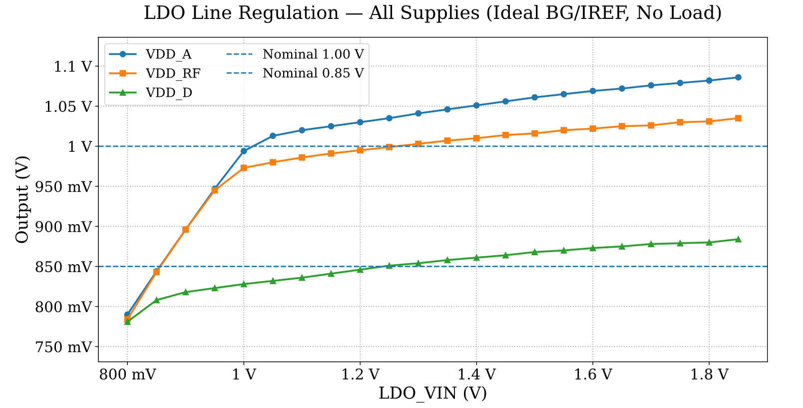
Measured performance
Line regulation
Load regulation
Current Reference
Distributes 2 uA current reference to other blocks, includes a start-up circuit.
Parasitic extraction results:
- Typical conditions yields reference current ranging from 1.98 uA to 2.4 uA (~20% variation)
- Large variation with corners
- Worst case: ff_hot at 3.04 uA
Bandgap Reference
The Bandgap Reference Circuit (BGR) can be splitted into 3 parts: startup circuit, 2-stage op-amp, and the core BGR circuit. There are 2 included RDACs for the temperature coefficient and output voltage (Vref) adjustment.
Parameters and simulated performance
| Parameter | Spec |
|---|---|
| Output, VBAT=1.6V | ~650 mV |
| Power Consumption, T=27C | ~1.8 mW |
| PSRR, f=1 MHz | ~58 dB |
| Layout Area | ~ 7,500 um² |
Core BGR Circuit
The temperature compensation coefficient is determined by the ratio of R3/R2, while the output voltage level is determined by the ratio of R4/R2, assuming R1=R2. R3 and R4 are eventually implemented as RDACS to enable tuning of temperature coefficient and output voltage shifting for LDO Vref supply.
2-Stage Op-Amp
A two stage opamp with Miller compensation and pole cancellation was used.
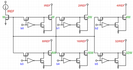
Utility Current DAC
Utility Current DAC schematic:
Parameters and simulated performance
| Parameter | Spec |
|---|---|
| Output @ 1.6 V | Up to 63 * IREF |
| Power @ 126 uA | ~50 uW |
| Input Current Range | [0.1 uA, 20 uA] |
| Load Voltage | ~ 150 mV |
| Average DNL Error | 1.73% |
| Overall INL Error | ~2 uA |
| Estimated Area | 800 um² |
- 6-bit binary weighted current mirror scaling
- Uses IREF input as LSB