Misc Notes
Hierarchical Design Flow Notes
We’ve seen big SoCs that include billions of transistors and thousands of human contributors. We’ve also seen that such chips include a wide diversity of tools and practices, varying between parts of the chip and phases of its design process. There is plenty of industry-specific alphabet-soup jargon to learn while getting comfortable with this process; first we’ll spend a moment on why we have it in the first place. A lot of this is technical, but just as much is essentially sociological. C++ father Bjarne Stroustrup was famously quoted putting this like so:
Coding is a human endeavor. Forget that and all is lost.
That idea is just as effective should we replace coding with designing or building. We’ve got a big thing we want to make, far bigger than any one of us could hope to build on our own in an amount of time we’d care to build it. How do we divy up this task, both in people and in time? What technical infrastructure can we (or our predecessors) put forth to help in this task?
Effective divisions of this labor for complicated systems have generally arranged its sub-systems into a tree-like hierarchy. Parallelizing work on higher (closer to the root) layers of the tree generally requires they include some form of abstract description of lower layers. These design-abstracts include the necessary information for integrating and using a sub-system, without necessarily including all of its implementation details. These abstracts are also commonly divided among different domains or disciplines. Some of the important chip-design disciplines include:
- Parametric, e.g. performance specs
- Physical, e.g. layout
- Behavioral
- Timing
The latter is specific to synchronous digital systems, of which our chip is (mostly) one. Its inclusion of a list at this high priority may seem out of place, and conceptually it may be. But static timing analysis is sufficiently integrated into our digital-compilation pipeline that we’ll need to know about it, just about as importantly as we’ll need to know about layout and Verilog.
This list of disciplines can (and does) get quite a bit longer in practice. There are associated hierarchical models for testability, electromigration, power integrity, and just about any other domain-general chip-design quality-metric we can think of. This shorter list will be our focus. (Most of the longer list would be overkill for low-volume academic chips anyway.)
Parametric Specs
For non-integrated electronic systems, e.g. those built on PCBs, the primary abstract-description format is the datasheet. These have been around a long time; long enough to precede PDFs, or computers to render PDFs for that matter. Nowadays the datasheet typically comprises all of the abstract information in one bundled PDF file. (In prior days it did the same, just on typed paper.) One perennial component of those datasheets is the parametric spec-table, for instance:

These spec-tables are probably how analog-brains most-commonly think of these abstract sub-systems. Sorting out how these sub-systems’ parametric specs combine into larger-systems parametrics can be more of less straightforward. Power consumption serves as a super-simple example: a system with sub-systems A, B, and C consumes power equal to the linear sum of the powers consumed by A, B, and C. Other metrics combine with more difficulty. Those of you who have studied RF circuits have likely needed to compute some of these more elaborate combinations, such as for noise, linearity, and offset.


From A Niknejad’s Advanced IC Design for Communications
While those metrics combine with more difficulty than a linear sum, their combinations are at least analytically tractable. Many other such combinations are not, and require dedicated programs or simulation models to measure.
Many of our systems will not have this analytical-tractable-combination property. It’s seemingly impossible, or at least highly impractical, to estimate their performance from such a table of sub-system metrics. Our CPU’s execution-time when running a benchmark suite will fall into this category. For such systems we’ll typically rely on simulation models instead.
Notably for now: these analytical sub-system parametric-models generally do not feed into our chip-compilation pipeline. The remaining disciplines we’ll cover, in contrast, are tightly integrated and required for it to run.
Abstract Layout and Its Typical Format, the LEF
The first such discipline we’ll review is physical layout. As in most disciplines, enabling integration of layout does not require its internal details, but only its exterior interface. These abstract layouts serve as physical-integration contracts, so that layers above and below them can proceed in parallel. On IC datasheets detailed internal layout is rarely (read: never) provided, as a simplified drawing of the IC outline suffices in its place:

On-chip, abstract layout generally includes things like:
- A cell’s dimensions, shape, and outline
- Its pins, their locations, metal layers, and sizes
- Some indication of where parent layouts may route through the internal volume of the block, versus where they may not
Our industry’s overwhelmingly most-popular format for layout-abstracts is the Library Exchange Format, a spelled-out acronym you’ll never hear again, because it’s universally said and prounced LEF (like “laugh”). LEF is an ASCII text-format. It has a handful of scoped definition features, such as its own concept of a “library”. For our discussion of hierarchical design and analysis, we’re really most interested in its module-analogous concept, which LEF calls MACRO. We can find an example LEF MACRO in our ChipYard repository, representing the ExampleDCO used in past UCB-chips’ PLLs. The ExampleDCO LEF-excerpt includes:
- The module’s outline via a
SIZEattribute - Each of the module’s (excerpted)
PINS, including their metal layers and sizes - A list of obstructions (
OBS), through which it insists parent layouts may not add further metals
VERSION 5.6 ;
BUSBITCHARS "[]" ;
DIVIDERCHAR "/" ;

MACRO ExampleDCO
  CLASS BLOCK ;
  ORIGIN 0 0 ;
  FOREIGN ExampleDCO 0 0 ;
  SIZE 123.936 BY 125.536 ;
  SYMMETRY X Y ;
  PIN VDD
    DIRECTION INOUT ;
    USE POWER ;
    PORT
      LAYER M5 ;
        RECT 3.024 121.536 3.8 125.536 ;
    END
  END VDD
  PIN VSS
    DIRECTION INOUT ;
    USE GROUND ;
    PORT
      LAYER M5 ;
        RECT 1.728 121.536 2.5 125.536 ;
    END
  END VSS
  # ...
  PIN sleep_b
    DIRECTION INPUT ;
    USE SIGNAL ;
    PORT
      LAYER M4 ;
        RECT 0.0 45.312 1.2 45.696 ;
    END
  END sleep_b
  PIN clock
    DIRECTION OUTPUT ;
    USE SIGNAL ;
    PORT
      LAYER M4 ;
        RECT 122.736 0.384 123.936 0.768 ;
    END
  END clock
  OBS
    LAYER M1 ;
      RECT 1.2 0.0 122.736 121.536 ;
    LAYER M2 ;
      RECT 1.2 0.0 122.736 121.536 ;
    LAYER M3 ;
      RECT 1.2 0.0 122.736 121.536 ;
    LAYER M4 ;
      RECT 1.2 0.0 122.736 121.536 ;
    LAYER M5 ;
      RECT 1.2 0.0 122.736 121.536 ;
    LAYER M6 ;
      RECT 1.2 0.0 122.736 121.536 ;
    LAYER M7 ;
      RECT 1.2 0.0 122.736 121.536 ;
    LAYER M8 ;
      RECT 1.2 0.0 122.736 121.536 ;
    LAYER M9 ;
      RECT 1.2 0.0 122.736 121.536 ;
  END
END ExampleDCO

END LIBRARY
A complete layout of the same circuit, in contrast, would include all of its internal detail: where diffusions and gates cross to form transistors, how internal signals are routed, and the like.
Abstract Timing and Its Typical Format, Liberty
Many of you will have seen static-timing analysis (STA) as a part of past digital circuits courses. It serves as a highly efficient means of verifying the physical-design of synchronous digital circuits, and is tightly integrated in a typical digital compilation pipeline. STA effectively transforms digital circuits’ primary physical-layer validation step into a combination of (a) graph analysis to find timing paths, and (b) relatively straightforward arithmetic to compute their delays.

Partovi, Clocked Storage Elements
For the same reasons as all of our other analyses, large systems will commonly invoke static-timing hierarchically. Module-level static-timing models are commonly stored in the Liberty format. They are often referred to as “libs” or “dot-libs”, and generally have the file-suffix .lib. That name often invokes plenty of confusion, since it’s just as likely to sound like a “library”, either in the binary-program sense or in the collection-of-circuits-and-related-stuff sense we often use in IC design. These Liberty-models are the same format typically provided as part of standard-logic-cell libraries.
Like LEF, Liberty is a text-based format. It has a handful of scoped definition features, such as its own concept of a “library”. For our discussion of hierarchical design and analysis, we’re again most interested in its module-analogous concept, which Liberty calls cell. A Liberty cell conceptually consists of:
- The cell’s pins, and all timing relationships between each pin.
- For combinational logic paths, these generally take the form of delays, specified in semi-tabular format across variables such as loading and input slew rate.
- For sequential pins and paths, these take the form of setup and hold constraints. These cells also generally include delay-style paths, for example from clock to output.
- The capacitive load presented by each pin
- The power-supply domains of each pin, and
- A handful of meta-information that will often help tools use the cell, or analyze larger blocks which use it.
- A common example is
leakage_power, which expresses cell’s idle-state power consumption in conditions dictated by awhenclause.
- A common example is
To our author’s knowledge there is no publicly available, comprehensive documentation of the Liberty format. I certainly am not an expert on its details, and don’t think I know anyone else who would claim to be such an expert either. Liberty’s text-based format and highly-loose documentation makes it amenable (or prone) to both simple scripts generating and manipulating cells, and just as often, to those scripts screwing them up in ways overt and subtle. From-scratch LIBs are almost always generated by timing analysis tools, whether for standard-cell library characterization or larger cell-level characterization.
The AND2 below will server as our simple example of a Liberty cell. You’ll note it includes:
leakage_powerfor each of its static states- Descriptions of each of its signal-pins,
A1,A2, andZ - The
pg_pinsandpower_down_functionsfor each output pin - An (excerpted) list of
timingpaths in thepin(Z)section. The section labeledrelated_pin: A1describes the delay fromA1toZ, including the table over two index-variablesindex_1andindex_2, defined off-screen
cell (AND2) {
  area : 0.4;
  pg_pin (VDD) {
    pg_type : primary_power;
  }
  pg_pin (VSS) {
    pg_type : primary_ground;
  }
  leakage_power () {
    value : 4.5;
    related_pg_pin : VDD;
  }
  leakage_power () {
    value : 2.0;
    when : "!A1 !A2 !Z";
    related_pg_pin : VDD;
  }
  leakage_power () {
    value : 5.0;
    when : "!A1 A2 !Z";
    related_pg_pin : VDD;
  }
  leakage_power () {
    value : 4.4;
    when : "A1 !A2 !Z";
    related_pg_pin : VDD;
  }
  leakage_power () {
    value : 6.4;
    when : "A1 A2 Z";
    related_pg_pin : VDD;
  }
  pin(A1) {
    direction : input;
    related_ground_pin : VSS;
    related_power_pin : VDD;
    capacitance : 0.000388307;
    rise_capacitance : 0.000388307;
    fall_capacitance : 0.000366013;
    internal_power () {
      when : "!A2&!Z";
      related_pg_pin : VDD;
      rise_power (passive_power_template_7x1_0) {
        index_1 ("0.0016, 0.0083, 0.0216, 0.0482, 0.1015, 0.2081, 0.4214");
        values ( \
          "-0.000169101, -0.000165176, -0.000168139, -0.000169215, -0.00017008, -0.000171007, -0.00017275" \
        );
      }
      fall_power (passive_power_template_7x1_0) {
        index_1 ("0.0016, 0.0083, 0.0216, 0.0482, 0.1015, 0.2081, 0.4214");
        values ( \
          "0.00024232, 0.000239247, 0.000241563, 0.000242498, 0.000242565, 0.000242863, 0.000242053" \
        );
      }
    }
  }
  pin(A2) {
    direction : input;
    related_ground_pin : VSS;
    related_power_pin : VDD;
    capacitance : 0.000448479;
    rise_capacitance : 0.000448479;
    fall_capacitance : 0.000428282;
    internal_power () {
      when : "!A1&!Z";
      related_pg_pin : VDD;
      rise_power (a_template_table_defined_elsewhere) {
        index_1 ("0.0016, 0.0083, 0.0216, 0.0482, 0.1015, 0.2081, 0.4214");
        values ( \
          "-0.000221115, -0.000217392, -0.000220049, -0.000221058, -0.000221394, -0.000221981, -0.000221396" \
        );
      }
      fall_power (passive_power_template_7x1_0) {
        index_1 ("0.0016, 0.0083, 0.0216, 0.0482, 0.1015, 0.2081, 0.4214");
        values ( \
          "0.000252858, 0.00023764, 0.000235796, 0.00023427, 0.000232813, 0.000231391, 0.000228648" \
        );
      }
    }
  }
  pin(Z) {
    direction : output;
    power_down_function : "!VDD + VSS";
    function : "(A1 A2)";
    related_ground_pin : VSS;
    related_power_pin : VDD;
    max_capacitance : 0.02642;
    timing () {
      related_pin : "A1";
      timing_sense : positive_unate;
      timing_type : combinational;
      cell_rise (a_template_table_defined_elsewhere) {
        index_1 ("0.0016, 0.0083, 0.0216, 0.0482, 0.1015, 0.2081, 0.4214");
        index_2 ("0.00012, 0.00054, 0.00138, 0.00305, 0.00639, 0.01306, 0.02642");
        values ( \
          "0.0117336, 0.0137303, 0.0170961, 0.0230851, 0.034629, 0.0574656, 0.103475", \
          "0.0133137, 0.0153002, 0.0186687, 0.0246761, 0.0362021, 0.0590866, 0.105057", \
          "0.0159362, 0.0179294, 0.021311, 0.0273291, 0.038871, 0.0617699, 0.107525", \
          "0.0191142, 0.0212184, 0.0246963, 0.0307626, 0.0423069, 0.0651475, 0.110877", \
          "0.0228423, 0.025173, 0.0289792, 0.0352166, 0.0467551, 0.0696063, 0.115304", \
          "0.027315, 0.0299445, 0.0342669, 0.0411978, 0.0531457, 0.0760411, 0.121886", \
          "0.0327368, 0.0358058, 0.0409214, 0.0490805, 0.0623833, 0.0862778, 0.132597" \
        );
      }
      // ...
So this gets complicated fast. But nowhere near as fast as eschewing the hierarchical representations and attempting to close timing on billions of paths at once.
Note the role of the process, temperature, and voltage conditions. SPICE-verified circuits can generally both (a) sweep the entire outer product of these conditions, and (b) expect their circuit performance to (usually) be relatively smooth functions of those conditions. Hierarchical timing descriptions, in contrast, generally enumerate each of a set of “PVTs”, or conditions at which their cell libraries are characterized in simulation.
A note on the origins of all these weird file-formats: our industry as it stands, and our partner EDA industry that generated most of this stuff, really grew into its current state in the 1980s. Creating custom text-based file-formats was cool then, I guess. As must have been writing custom parsers for them, and validators, and all. This was before the software industry collectively realized this was a pretty big waste of everyone’s time, and put all the data being shipped around the web into JSON, and all the configuration being shipped around the industry into YAML, TOML, and a few other markup-languages. It was before the prior revolution which decided the same thing, but instead put it all into more verbose XML.
So virtually every other file has its own self-defined, ill-documented, ASCII-based schema. For example the files which map GDS layers to their purpose and description will look something like:
DIEAREA ALL 100  0

M1     LEFPIN,LEFOBS,PIN,NET,SPNET,VIA 31       0
# ...
M9     LEFPIN,LEFOBS,PIN,NET,SPNET,VIA 39       60
M1     VIAFILL,FILL            31    1
# ...
M9     FILL            39    61
# ...
# ... (note these "comments" aren't actually supported)
# ...
VIA1     LEFPIN,LEFOBS,VIA   51       0
VIA1     VIAFILL         51    1
NAME     M1/PIN          131    0
And they will have a typical file-extension of: nothing. Such is our field; complain about it, or do something about it.
Behavioral Models
Verifying our digital systems will generally require some form of whole-system integrated simulation, often requiring interaction with an analog sub-system. In this context, the parametric spec-table ceases to really describe the analog circuits very well; we need a better indication of what they do, or in other words, how they behave. For example, here’s a very-analog circuit that appears over-and-over in modern SoCs: Banba’s sub-1V band-gap reference.

Banba, A CMOS Bandgap Reference Circuit with Sub-1-V Operation
We can imagine a larger parametric table of spec-data accompanies each of these circuits: its power-supply rejection, start-up time, power consumption, and the like. But what level of detail would an SoC-level simulation need of this circuit? Would we care, or want to spend the time reacting to these subtleties of its performance?
The version pictured above from Banba’s original journal article includes a power-on-reset input and no enable input. We can instead imagine a version with an input signal (enable) that tells it when to turn on and off, an output reference voltage, and no other IO. And we can imagine a simple integration-targeted behavioral model that captures this, and nothing more:
module bandgap (
  input en,
  output vref,
);
  assign vref = en;
endmodule
Note this simplest model eschews most of the circuit’s design details, but retains one in full: its IO interface. These pin-compatible models are crucial to use in digital simulations, which generally fail if pin-incompatible modules are included.
The behavior captured by these models need only be as detailed as the larger system needs of them. If an indication of whether a module is enabled or disabled suffices, use it. Add detail only where it helps. The amplifiers in our RF transceiver will have a long list of performance criteria regarding their noise, linearity, power, offset, and all sorts of analog-isms that will require time-consuming simulations to evaluate. Instead in integration sims, something as detailed as an “and-gate” model will often suffice:
module opamp (
  input inp,
  input inn,
  input bias,
  input en,
  output out,
);
  assign out = en & bias & inp & !inn;
endmodule
Note in both the bandgap and opamp cases, ports which hold analog values in our ultimate implementation are dumbed-down to simple logic values. These simplifications require careful choice of module boundaries and interfaces. Feedback loops which traverse multiple modules, and especially multiple simulation-domains, require the most simulated-attention. As a general point of advice: avoid them.
Now, how can we tell whether these simple models accurately capture the behavior of the taped-out implementations? In general, this is hard, and our industry doesn’t have a foolproof (much less easy) answer for it. For digital and structural circuits, formal verification tools aid in such comparisons (in addition to those against even more-abstract models). For analog and custom circuits (e.g. your standard cell library) these equivalences are more commonly established through (a) targeted simulation, and (b) human review. Reducing the scope of the circuits behaviorally-modeled is therefore invaluable in making these simulations and reviews more efficient and tractable.
There are of course many steps in-between these maximally-basic “and-gate” models, and fully featured ones which capture detailed performance metrics. A few relevant tools, in increasing order of simulation complexity, include:
- Real-number modeling in SystemVerilog
- Real-valued wire-types in SystemVerilog
- Analog and mixed-signal description languages such as Verilog-A and Verilog-AMS
- Mixed-mode simulation, including a combination of discrete-event Verilog and transistor-level SPICE
The latter half of this list increases in sim-time very quickly. It’s worth a moment to consider just how different these can be, by thinking about what each simulation model is actually doing. Verilog simulation operates on a discrete-event paradigm. Signals are piecewise-constant in time. A set of execution tasks, such as those annotated by always and initial delimiters, runs in response to their changes. The typical Verilog simulator is then essentially a weird C compiler, paired with a small (and also weird) run-time to tell these functions when to run.
The SPICE runtime is a whole different ballgame. SPICE’s model of computation is essentially solving the combined system of (a) Kirchoff’s current and voltage laws, and (b) the very-elaborate modern device-model equations. This system is both non-linear and time-varying, requiring a combination of iterative (i.e. “guess and check”) tactics and numerical integration. Modern device models, such as the BSIM4 devices used in our project, will include multi-thousand-line evaluation procedures, per transistor, per time-step, per guess. So it’s a lot of math.
In summary:
| Language | How Simulations Work |
|---|---|
| (System) Verilog | * More or less a C compiler * Discrete-event runtime tells which “functions” when to run |
| SPICE | * Lots of non-linear matrix math * Bazillion-line transistor models |
| Verilog-A | * Same non-linear matrix-math * Your code replaces those transistor models |
| Verilog-AMS | Just a merge of Verilog and Verilog-A, with some glue in between |
It’s difficult to find super-rigorous apples-to-apples comparisons between the computational complexity of these simulation paradigms. One such study, appraising models of the same phase-locked loop, found over an eight order of magnitude such difference:

Igor Ikodinovic, Modeling for Analog and Mixed-Signal Verification
For a sense of scale: were the Verilog simulation at right to take one second, this would imply the SPICE-level simulation would take over three years. It’s hard to say how well this maps onto the author’s own experience, since in practice, the three-year simulations just don’t get started in the first place. (And for clarity: there are certainly PLL SPICE simulations that take far less time, although still a long time.)
The take-away should nonetheless be: there are orders-of-magnitude differences in how costly these different simulation-paradigms can be. Our chip will be sufficiently complicated that the slower ones will take far longer than the time we have to design it. Our only realistic alternative is to create these more-abstract models.
Implications for Building Hierarchical Systems
Unlike the parametric-spec abstracts, those for behavior, physical layout, and timing generally are included in the compilation pipeline for every layer of hierarchy above them. Each of the primary digital construction tools uses some combination of them while inline-analyzing its input and producing its ultimate output.
The abstract views for timing, layout, and behavior also have a lot of information in common, which generally must be self-consistent between them for any of these tools to coherently work. Particularly, all three include each module’s port list. Setting these port-interfaces and their behavior then becomes a crucial early task for a hierarchical design process. In contrast to a bottom-up process in which parametric specs drive leaf cells, which drive their parents (both internally and at their interfaces), a hierarchical process requires definition of each sub-system’s abstract views, generally in order of:
- Interface
- Behavior
- Layout
- Timing
The early requirements for interfaces and behavior also aligns with a mixed-signal chip-style, in which a set of digital logic configures and collaborates with a set of deeper-nested analog circuitry. Settings, configuration registers, calibration steps, and the like appear “from thin air” in MATLAB and similar models of these blocks, but typically require someone, often someone else, to design into silicon.
This course’s design process won’t adopt the full ten-billion-transistor flow, but will be hierarchical. So we’ll need a similar set of priorities to enable upper-layers and lower-layers to work in parallel: define interfaces and behavior early, and implement against them to follow. Defining interfaces early is a crucial part of this process. Several of our upcoming design milestones will focus on this hierarchical division of labor.
Embedded Bring-Up Notes
Once all of this design-work is done, it’ll turn into actual, real-life, physical pieces of silicon. Question is: then what?
We’ll need lots of specialty lab equipment for testing our RF transceiver, and for powering up our chip in the first place. But getting our chip to do much of anything will require interacting with our processor. A central step will be: how does our processor get its code? And more importantly for now: what do we need to design into the chip to support this?
More elaborate systems such as a PC or smartphone have a multi-step boot process, starting from a minimal set of boot code, working often in several steps up to loading an operating system from disk or flash, which in turn loads any further applications. Processor-systems like our own, in contrast, are often referred to as embedded, in the sense that while they run code, its function is not immediately user-visible or editable. Unlike on their PC or smartphone, users don’t have much control over what code runs in these embedded systems, potentially save for infrequent version-updates. Examples abound throughout your life - many of which are sufficiently embedded that you may not realize a processor is even present. (Inside a remote-control or electronic greeting card, for example.)
Much of our research infrastructure is designed to generate processor-based systems which range in scale from these embedded-sizes to large, high-performance, multi-core systems. (Our chip is at the low end of this spectrum.) The Berkeley Architecture Research test-environment is designed for some of the more elaborate cases, and requires some correspondingly elaborate setup.

Here “Beagle Chip” is the researcher-designed custom IC, and everything else is its test and bring-up environment. Program-loading and interaction runs through a large FPGA, which in turn runs its own custom soft-CPU core, running its own custom flavor of Linux. “Your” computer, i.e. the laptop you type the code into, is the “Host x86” box at left.
By emedded standards, this is a lot of stuff - particularly all the FPGA-programming parts. (Plus a VCU118 costs a few grand.) Most smaller systems can get by with simpler fixed-function programming and debug hardware, with much lower programming-burden and costs often in the hundreds or even tens of dollars. These devices generally aim to support either or both of:
- Program Loading, often just called programming - i.e. downloading the program onto some in-system non-voltatile memory-store
- Debugging - adding the capacity to interact with a running program, with capabilities such as inserting breakpoints, inspecting the code and system state, directly editing memory and/or register data
The test-infrastructure for these setups then generally consists of:
- “Your” computer, where the code gets written and compiled
- A little widget-board that plugs into it, typically via USB
- A connector between that widget and a (somewhat) standard interface on the chip
For example:
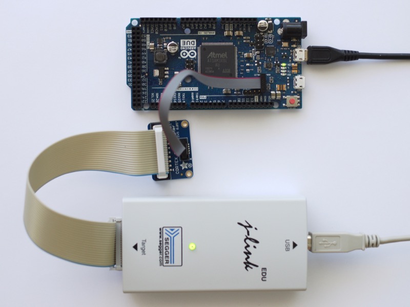
A common embedded-programming and debug rig, including an Atmel microcontroller board and SEGGER JTAG widget. In this case, as in many, the widget-board is encased in the plastic box labeled “Segger” and “J-Link”. The smaller, bare board is just a connector-size-shrinking adapter.
Our chip will include two such standard interfaces: JTAG and SPI. JTAG is frequently used for a wider range of things, but in this context we’ll examine its use for embedded debug.
Processor-Specific Debuggers
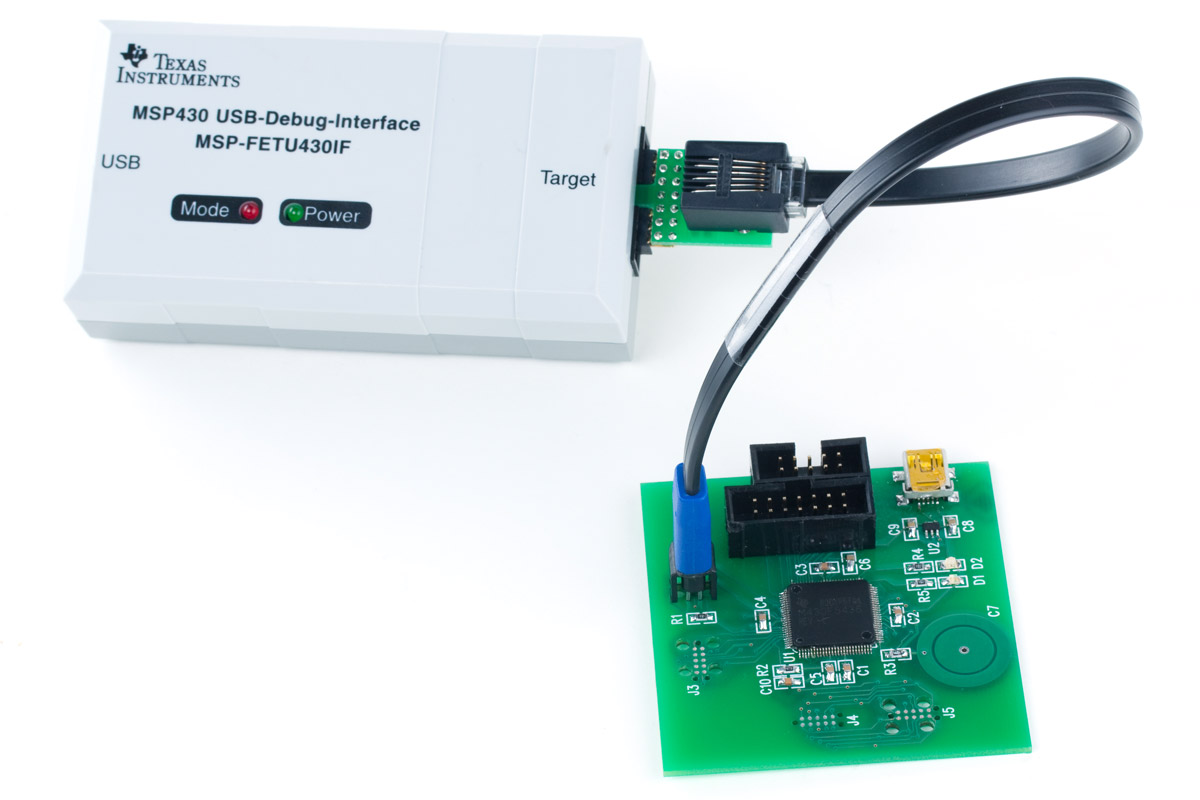
For most of embedded-system history, most embedded processors have used custom, closed-source ISAs. This generally requires such processors include a compiler chain and associated tools for interactive with a host-PC, where the code gets written and compiled. Many of these devices also include custom-designed programming and/or debug interfaces, to reduce wire-count, or add features, or for whatever reason the designers didn’t like the standard ones. The TI MSP430 programmer pictured below is one such example. Unlike ours, many such processors also include on-die non-volatile memory (e.g. embedded flash), and the capacity to program that memory in-circuit. This often unifies the program-loading and debug interfaces into one.
Many of the Arduino family of boards, which feature Atmel microcontrollers, use a similar custom-debug-bus internally, but include on-board circuitry (in the form of a second microcontroller) to expose their programming interface via USB. (Think of this as the board and plastic box above merged into one.)

Arduino’s Uno board, featuring an ATmega328P microcontroller
In this case the chip has a custom debug interface, and the board reconciles it to a standard one, USB.
Standard Programming & Debug Interfaces
Our own chip is as open-source as we can make it, and won’t use or define any custom debug interfaces. Instead for sake of compatibility and reusability, we use industry-standard interfaces: SPI and JTAG. Many embedded processors with similar goals adopt a similar approach, and benefit from a suite of common tools which use these interfaces. Among the most popular are Segger’s J-Link family, one of which was pictured in our first example, and a smaller cousin below.

A Segger JTAG Board
These boards and boxes are in wide industry circulation. Some companies go as far as open-source publishing their libraries making use of the Segger boxes.
Embedded-system boards such as SparkFun’s RED-V use solely standard interfaces for programming and debug - conveniently the same JTAG and SPI included on our chip. Its schematic shows it routes those two interfaces to external (and semi-standard) connectors. For JTAG, the little-widget functionality is built-in, via a custom-programmed ARM processor and its USB connection.
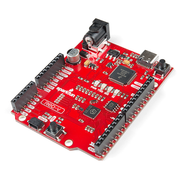
SparkFun’s RED-V Board, featuring a SiFive RISC-V SoC not all that dissimilar from our own. Note this includes a USB-JTAG programming widget in the form of a custom-programmed ARM Cortex, right on the board.

Particle’s USB-JTAG Debugger
Standard Programming (Without Debugging) Interfaces
Embedded processors without on-die non-volatile memory (such as ours) commonly store their program and persistent data in external flash chips, commonly connected via SPI. The processor’s boot-code will then quickly read the program from the SPI flash into program memory to begin program execution. These off-die program stores offer a bit easier opportunity for program loading, especially since the SPI interface is standard and widely used. This largerly just requires holding the processor in reset while a programmer-widget loads bits into the flash via SPI. Such SPI-compatible programmers, such as those from TotalPhase are often quite low-cost and low-effort to set up.

A SPI flash programmer. An out-of-circuit version is shown here; similar devices commonly program in-circuit as well.
Of course a primary downside to the SPI-based program loading is that SPI is largely incapable of the kinds of in-circuit debugging one can access via JTAG.